• From concept
    to market


  • Creating
    solutions

About Us

Company Profile

Modern high-tech companies and startups are reliant on the ability to launch novel ideas in nano- and micro-device based technologies from their conception to cleanroom prototyping and manufacturing – at an affordable cost and within a short timeframe. Often the entrance into cleanroom-based R&D is complicated by prohibitively high costs due to overly-complex fabrication flows with low quality and yield. Efficient design processes, smart benchmarking and elegant fabrication solutions enable businesses to quickly and affordably assess the feasibility of their road-maps and next-generation ideas.

Nenso Solutions was founded in 2018 by a team of nanofabrication experts with a combined experience of more than 30 years in high-precision nanofabrication and low-noise quantum measurements. Our experience allows us to guide emerging ideas and initiatives in a number of fields ranging from microchip sensors, to bio-physics, to the expanding market centered on nanophotonics and quantum technologies at significantly lower costs. Our services include appraisals of nanofabrication facilities, counseling on the feasibility of their methods and help with the identification of intellectual property within the microchip design and manufacturing. Nenso Solutions aims to consult on new projects from idea to chip, while helping innovators to retain control and knowledge of their innovations.

Design

Nano-Fabrication

Prototyping

Development

Want to know more?

The people behind Nenso

Team

Simon Groeblacher

Dr. Simon Gröblacher

Director

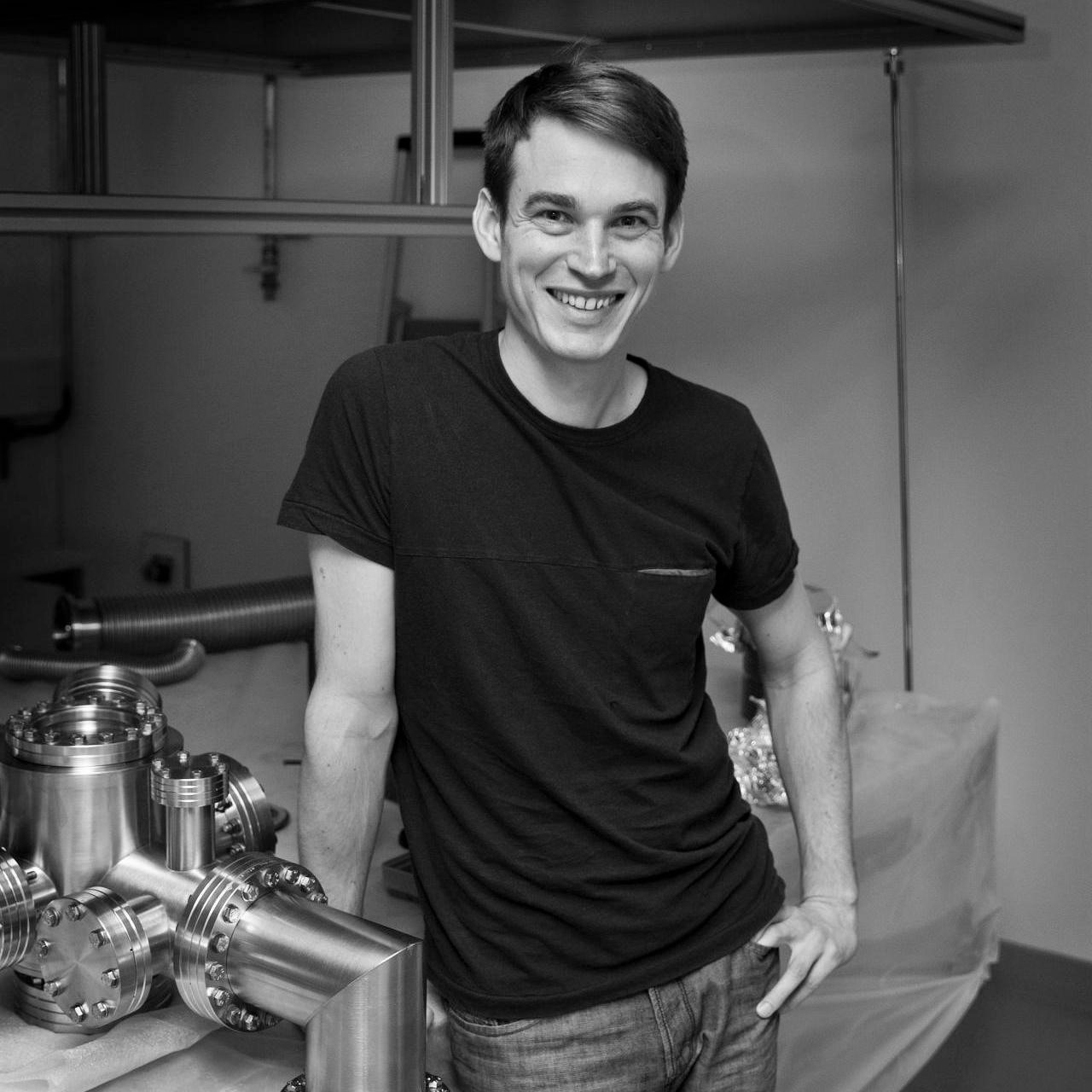
Professor of Quantum Physics in the Department of Quantum Nanoscience at Delft University of Technology, Netherlands and founder of Nenso Solutions. Simon is running one of the world’s leading research groups in microchip quantum technologies, and has extensive expertise in micro- and nano-fabrication, as well as quantum optics. He has been consulting biotech & nanophotonics initiatives on bringing microchip architectures to the market with efficient, low-cost, and high-yield nanofabrication. His work has been published in renowned journals, including Science, Nature, Nature Physics, as well as Scientific American. Before moving to Delft, he received his Ph.D. in physics from the University of Vienna, Austria and then spent 3.5 years as a Marie Curie fellow at the California Institute of Technology.

Job opportunities at Nenso

Careers

Job opening

We currently have no vacancies. Please check back here periodically for future openings.

Recent Work

Overview of some of our recent work

Nanotechnology featured on cover of Scientific American

July 2018 Does quantum mechanics have a size limit? Our novel fabrication techniques and designs of nano-photonic devices allow us to realize microchip resonators which are sensitive enough to probe the boundary between the quantum world of atoms and the classical world we see around us every day.

Read more

High-precision fabrication enables entanglement of massive systems

April 2018 Our state-of-the-art in-house fabrication of silicon-on-insulator (SOI) allows us to observe entanglement between two macroscopic mechanical objects for the first time. This high-precision SOI nano-fabrication enables us to realize silicon nanostructures which are indistinguishable at the quantum level.

Read more

Record-Breaking Sensors using Next-Generation Fabrication and Design

April 2016 By looking at the physics of how we make microchips, we have been able to engineer the world’s most sensitive micro-mirror force sensors using silicon nitride membranes. This has been enabled by some of the cleanest, high-performing nano-fabrication to date.

Read more

Cover of Quanta Magazine

June 2018 Nenso co-founder, Simon Gröblacher, and his research with silicon-on-insulator chips are featured in Quanta Magazine, where he highlights his achievements in creating quantum technologies using nano-scale mechanical devices combined with ultra-low loss photonics.

Read more

Integrated Photonics make the cover of Optica

December 2018 By developing high-yield cleanroom processes for silicon nitride, we have been able to demonstrate the first interaction of integrated nano-photonics devices with an optically levitated object. This technology has allowed us to place the photonics platform directly on the tip of an optical fiber with very high-fidelity.

Read more

Superconducting sensors highlighted in Scientific American

August 2018 Using our manufacturing techniques, we produce microchips sensitive enough to measure movements on the femtometer level – a scale usually reserved to describe the radius of protons. We combine this state-of-the-art capability with superconducting circuits to explore fundamental physics that has thus far been out of reach.

Read more

Get in Touch

Contact

Lorentzweg 1
2628CJ Delft
The Netherlands